Samsung unveils zHBM memory stacked directly atop AI accelerators at FMS 2026
Samsung unveiled zHBM, a memory design that stacks high-bandwidth memory directly atop AI accelerators, at the FMS 2026 conference, targeting roughly 8x HBM5 performance by 2029.
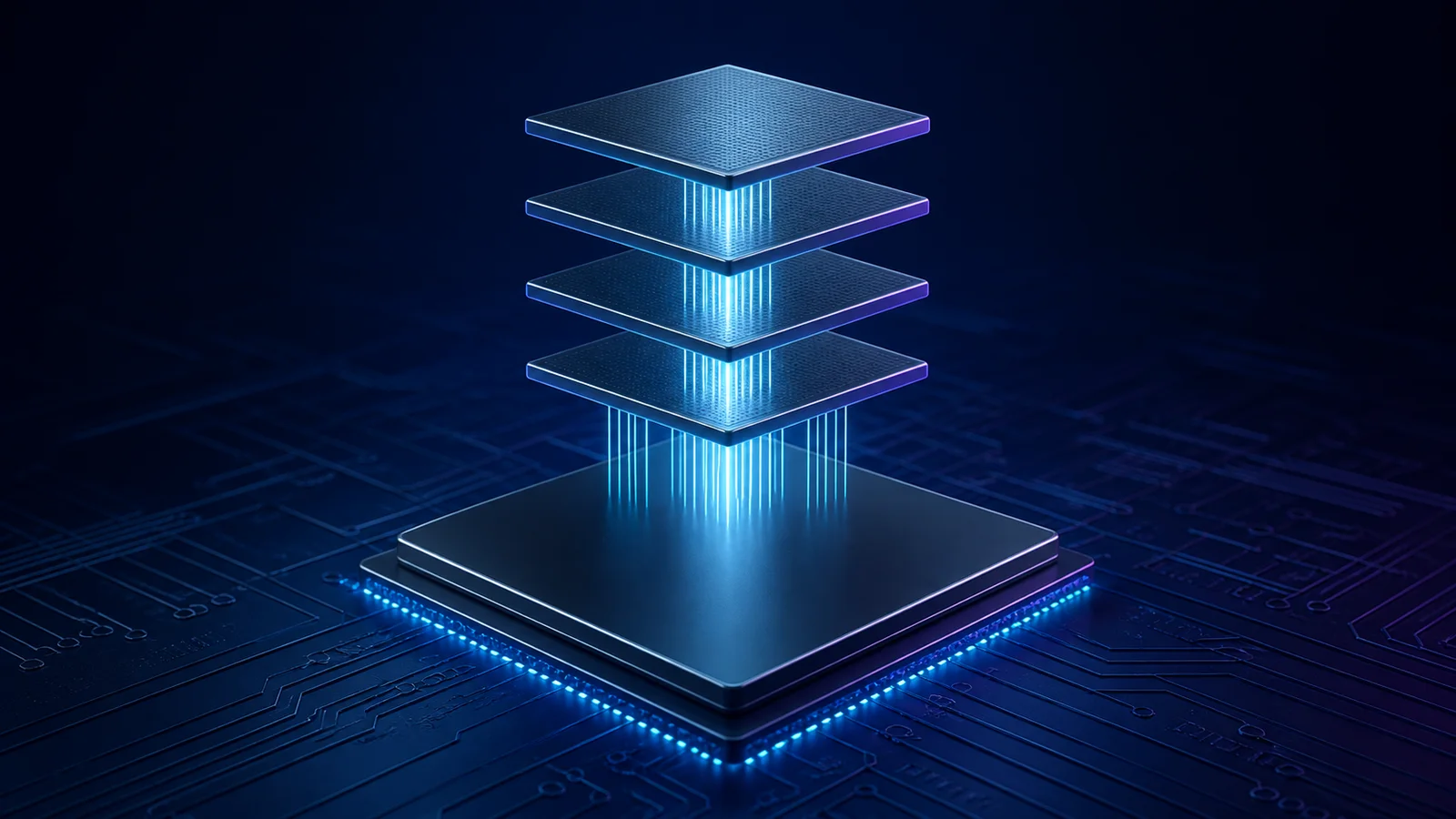
Samsung Electronics unveiled zHBM, a memory architecture that stacks high-bandwidth memory directly atop AI accelerators, at the Future of Memory and Storage (FMS) 2026 conference in Santa Clara on August 4, 2026. Samsung says the design is targeted for around 2029.
The company claims zHBM will deliver roughly eight times the performance of HBM5, with more than 10 times the density and triple the energy efficiency, according to its FMS 2026 announcement. Those are company projections for an unshipped part and have not been independently verified.
Placing memory on top of the processor, rather than next to it, shortens the distance data travels, the bottleneck that increasingly limits AI accelerators more than raw compute does. Samsung also showed zNAND-O, an edge-AI NAND architecture in four- and eight-layer versions built for low latency.
Its third concept, V10 BV-NAND, is what Samsung calls the industry’s first NAND enabled by wafer-bonding, with more than 400 layers and about 58% higher density than the prior V9 generation. It arrives 13 years after Samsung’s first V-NAND chip in 2013.
Alongside the concepts, Samsung displayed shipping product: HBM4E running at 16 gigabits per second per pin with 4 terabytes per second of bandwidth, which began sampling in May 2026, plus its HBM5 and LPDDR5X-PIM lines.
The roadmap is a statement of direction more than a shipping schedule. zHBM’s 2029 target leaves years for rivals SK Hynix and Micron to respond, and for the performance claims to be tested in real accelerators.
More news

DRAM and HBM capacity for all of 2027 is reportedly sold out to AI buyers
SK hynix commits $38 billion to two new AI-memory fabs

Micron lifts planned US chip investment to more than $250 billion through 2035
 Dmytro Spodarets·Jul 9, 2026