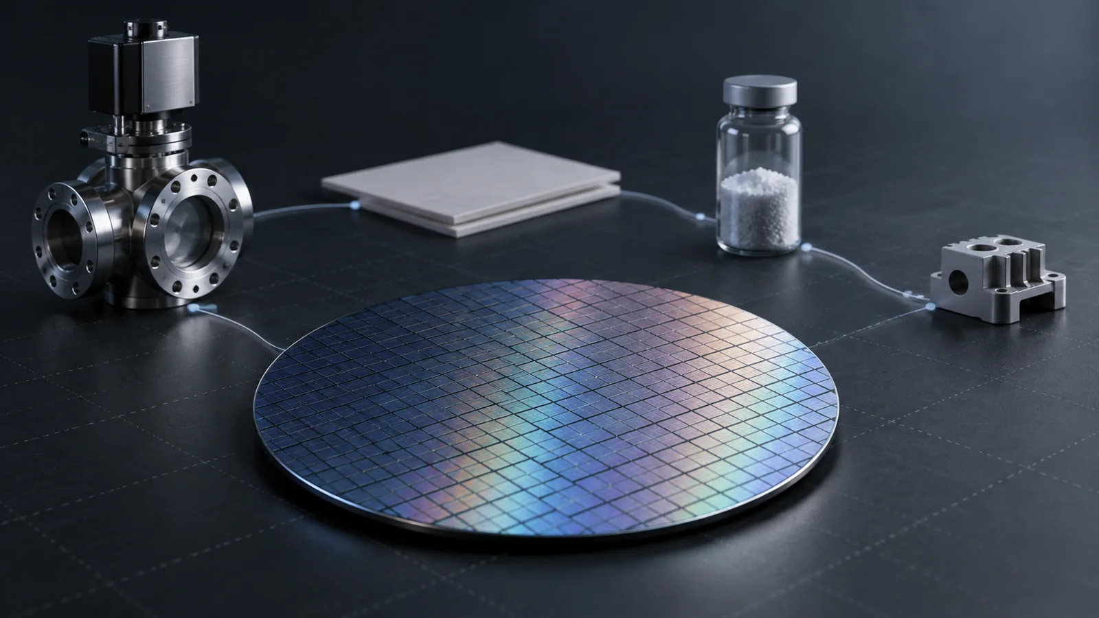
IBM plans early 7-angstrom nanostack design kit for 2027
IBM Research plans an early R&D process design kit for its 7-angstrom nanostack architecture, with availability targeted for the first quarter of 2027.

IBM Research plans to make an early research-and-development process design kit available for its 7-angstrom nanostack transistor architecture in the first quarter of 2027. The early kit is intended to help chip designers, electronic-design-automation vendors, equipment suppliers and researchers evaluate the architecture before widespread adoption.
IBM said the initial PDK will not include every model found in a mature commercial kit. The company expects the first version to include sample standard-cell libraries for logic functions and a sample SRAM design. Circuit designers could use those resources to test placement and routing, create early block-level layouts, and assess potential density and power-performance characteristics.
The planned release is a research and collaboration resource, not a production-qualified process. It does not establish foundry availability, customer tape-outs, yield or volume-manufacturing readiness. IBM did not provide a specific release date, access terms, pricing, licensing details or names of early collaborators.
Nanostack places n-type and p-type devices above and below one another rather than side by side. IBM said this three-dimensional arrangement changes circuit layout and introduces resistance, capacitance, thermal and device-interaction questions. The company uses 7 angstrom, or 0.7 nanometer, as a node label for the technology, not as one exact physical feature dimension.
A 2025 IBM Research paper projected about 50% area scaling, about 50% higher performance at the same power, or about 70% lower power at the same performance compared with IBM’s 2-nanometer node. Those figures are research projections, not benchmarks from shipping products.
IBM’s June 2026 technology announcement said the architecture had been experimentally validated through ultra-thin dielectric bonding, dual-channel engineering and functional CMOS inverter operation. The company separately said it saw a path to nanostack production within five years, a projection distinct from the first-quarter 2027 plan for an early research PDK.
More news
TSMC revenue rises 41.2%, with Q4 forecast at $52.3-$54.3 billion

US chip and AI-infrastructure stocks slide after inflation report
IBM and Siemens pair chip research with design software